Three Level Voltage Sourced Neutral Point Clamped Inverter
3-Level Neutral Point Clamped (NPC) inverter is one of the DC/AC converters with partitioned dc-link by diode clamps. The diode clamps are located such that each phase voltage is produced with respect to neutral point, which is actually the mid-point of dc-link. Since each phase voltage is produced with respect to neutral point (Z), the line-to-line voltages form a balanced three phase set for the load. Dc-link voltage is distributed such that two equal valued capacitors share the total dc-link voltage. For the three level operation there will be two capacitior to share the dc-link, meaning that each capacitor has voltage value E which is half of total dc-link voltage value.
With the changing switching schema each phase voltage (phase - neutral) can have three different voltage level. One of them is called P state, for this state corresponding phase has a voltage level of E. The second state is called O state, which corresponds to zero voltage on a phase. The last state is called the N state which corresponds to -E voltage on a phase. Since each phase voltage has three levels, the line-to-line voltages has five different voltage levels, namely +2E,+E,0,-E,-2E. With this voltage kind of voltage waveform, one can easily say that the most dominant voltage harmonic for this scheme should be larger than 10th harmonic. In addition to that information, naturally the voltage harmonics may lay around switching frequency and its integer multiplications. This kind of topology gives us lower dv/dt values than the traditional 2 level inverters with same dc-link value. However, one of the most challenging drawback is that the user should keep the upper and lower side capacitor voltages the same. The three level NPC topology is as shown in figure 1.
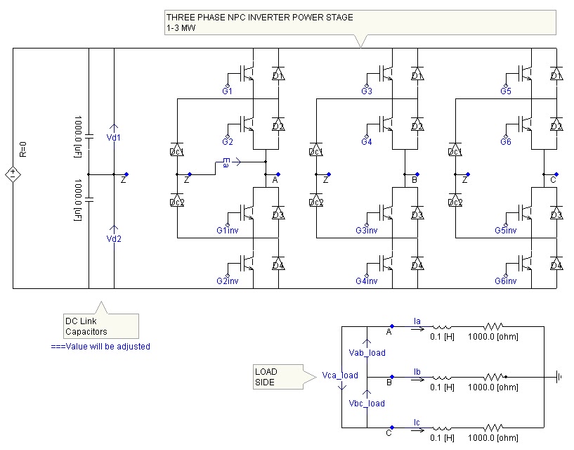
Figure 1 : 3 Phase NPC
Space Vector Modulation
Space Vector Modulation (SVM) technique is a bit more complex and challenging method than carrier based Pulse Width Modulation (PWM) techniques. To introduce SVM, let me remember some points about three phase systems. The three phase voltages at any instant ,actually, forms a space vector which is rotating around cartesian coordinates with an angular frequency 2*pi*f, f being system frequency. This space vector has a constant magnitude and its phase changing in time with the integral of angular frequncy stated. Please think that an observer sitting on the origin of cartesian coordinates sees this space vector as I stated before. What about an observer on a frame which is rotating with the same angular speed with the space vector? Actually the observer in synchronously rotating frame sees this vector space as constant in time. Knowing these concepts, our controller should be like an observer sitting in a fixed frame on cartesian coordinates. Suppose our observer has two point of views which are direct and quadrature axes. The instantaneous values of direct and quadrature axes represents the direct and quadrature components of the Space Vector for the 3 phase voltage. We are using a transformation called Clarke transformation (or alpha-beta transformation) in order to create a 2 phase representation of 3 phase voltage such that their space vectors coincide each other.
Space Vector Modulation technique creates a fixed valued reference space vector which is rotating with angular frequency of w. And to use this technique, the whole space is divided into 6 sectors and each sector is divided into 4 regions for 3-level operation. The corresponding divisions are shown in figure 2.

Figure 2 - Space Vector Modulation Divisions
Note that each position in dq space is represented a voltage state for phases a,b and c. For example Sector 1, Region II is enclosed with three space vectors 100(V1),210(V7) and 221(V2), meaning ONN,PON and PPO. To get a reference space vector using these three vectors in Sector 1 - Region II, these three vectors states should be applied some defined time intervals of Ta,Tb and Tc respectively so that the following equation holds. The time intervals Ta, Tb and Tc are called Dwell Times.
Vref * Ts = V1 * Ta + V7 * Tb + V2 * Tc , where Ts is switching period
Using our fixed space vectors, we can form any reference vector at any instant. By this way, for every period Ts we should calculate the direct and quadrature componenets of reference vector and find in which sector and region the reference vector lies. After we find the exact location of reference vector, we know which vectors are used for composing a reference for the corresponding section and region; thus, if we apply these vectors with the duration of calculated Dwell Times, we can form the required reference space vector. The calculation of Dwell Times are stated below in figure 3;

Figure 4: Dwell Times Formulas
In figure 4, Dwell Times calculations are stated, in these equations theta value will be the angle of corresponding sector and it must be between 0 and 60 degrees. The theta value for each sector is as stated below;
theta_Sector = theta_Reference - (Sector_Number - 1) * PI / 3
Also for the formulation in Dwell Times, there is another variable called modulation index, Ma. This modulation index is used for creating a reference with different magnitudes.
Ma = sqrt(3) * Vref / Vd , where Vd is DC-LINK voltage
0 <= Ma <= 1 , range of modulation index
Spece Vector Modulation Sequence Design
In previous sections, I mentioned how reference space vector is composed and how we can realize it using Dwell Times. After calculation of Dwell Times, one can ask that in which sequence we can apply the space vectors. This is actually one of the important parts of control system, because switching sequence determines some key points like even voltage distribution of dc link capacitors or elimination of even harmonics.
At the beginning, I said that there are 3 levels for each phase at any instant and since we have three phases, there are 27 different switching state for the inverter. All of this states corresponds to a space vector in figure 1. These space vectors are used to form the reference space vector which is rotation at a speed of w and has a constant magnitude which is determined by the modulation index Ma. Actually, some of the states corresponds to the same space vector. The whole table for the space vectors are as stated in figure 5.

Figure 5 : Space Vectors
I will mention one of the switching sequences called Seven-Segment switching sequence, which is actually the one I used for my application. The switching sequence is shown in figure 6.

Figure 6 : Seven-Segment Switching Sequence for Sector 1 - Region IV
Figure 7 represents the locations of Space Vectors.

Figure 7 : Space Vector Positions
The Inverter Results
PSCAD Simulation with topology in figure 1.
Ma = 1
frequency = 50 Hz
For SVM Control Block FORTRAN codes contact me from emredurna@gmail.com
PSCAD Simulation with topology in figure 1.
Ma = 1
frequency = 50 Hz
For SVM Control Block FORTRAN codes contact me from emredurna@gmail.com

Figure 8 : Output Voltage and Current Waveforms

Figure 9 : FFT for Vab/Vd for load side
REFERENCE : WU, B. High-Power Converters and AC Drives. 2006
Amazon
BetterWorldBooks.com - http://www.betterworldbooks.com/9780471731719-id-9780471731719.aspx
Abe Books - abebook.com - http://www.abebooks.com/servlet/BookDetailsPL?bi=9562576598&searchurl=sts%3Dt%26tn%3Dhigh%2Bpower%2Bconverters%2Band%2Bac%2Bdrives%26x%3D-843%26y%3D-95
BN - Barnes&Noble - barnesandnoble.com - http://www.barnesandnoble.com/w/high-power-converters-and-ac-drives-b-wu/1100521019?ean=9780471731719
BAM - booksamillion.com - (hardcover) http://www.booksamillion.com/p/High-Power-Converters-AC-Drives/Bin-Wu/9780471731719?id=5642034522726
(e-book) - http://www.booksamillion.com/p/High-Power-Converters-AC-Drives/Bin-Wu/Q7268713?id=5642034522726
BetterWorldBooks.com - http://www.betterworldbooks.com/9780471731719-id-9780471731719.aspx
Abe Books - abebook.com - http://www.abebooks.com/servlet/BookDetailsPL?bi=9562576598&searchurl=sts%3Dt%26tn%3Dhigh%2Bpower%2Bconverters%2Band%2Bac%2Bdrives%26x%3D-843%26y%3D-95
BN - Barnes&Noble - barnesandnoble.com - http://www.barnesandnoble.com/w/high-power-converters-and-ac-drives-b-wu/1100521019?ean=9780471731719
BAM - booksamillion.com - (hardcover) http://www.booksamillion.com/p/High-Power-Converters-AC-Drives/Bin-Wu/9780471731719?id=5642034522726
(e-book) - http://www.booksamillion.com/p/High-Power-Converters-AC-Drives/Bin-Wu/Q7268713?id=5642034522726


